Chapter One Link to heading
In our discussion of the “Lithography Machine Battle,” we mentioned that Nikon and IBM were betting on EBDW (E-beam Direct Write, also known as EPL or Electron Beam Projection) when crossing the 193nm threshold.
The wavelength of a 100KeV electron beam is only 0.004nm, which provides a much greater resolution advantage compared to EUV. Additionally, electron beams can be used with mature magnetic lenses, unlike EUV which requires reflective mirrors.
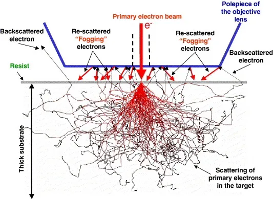
However, due to the Coulomb effect between electrons causing electron beam deflection and the scattering atomization effect shown in the figure below, it is difficult for electron beam lithography to simply increase current to improve efficiency.
The first generation of Nikon’s EPL produced 60nm wafers with only 7-10 wafers per hour. According to Tennant’s fifth power law, the efficiency of producing 15nm wafers will decrease to only 0.1%, and producing one wafer per day would be considered decent.
Although EUV is also valuable in energy, its efficiency is much higher than that of electron beams, which write one pixel at a time, because it scans an entire field of light in one go.
Electron beam technology is only applicable for low-volume products such as masks, as well as for applications such as wafer inspection and repair due to its low efficiency.
Multi-beam technology (using an array of thousands or even hundreds of electron guns) appears to have higher theoretical efficiency. However, the technical difficulty is significantly increased, and the smaller the pixel, the more electron beams are needed for each wafer, resulting in a bottomless pit of cost.
However, some advantages of multi-electron beams convinced Dr. David K. Lam, the legendary founder of Lam Research.
Chapter Two Link to heading
Lam Research has been translated as “La-mu Research” in Chinese, which is as fun as Toyota being translated as “dragging oil tower”. Lam is the pronunciation of the surname “Lam” in Cantonese Pinyin, and this translation is prevalent throughout Southeast Asia.
Mr. Lam was born in China and worked at Texas Instruments and Hewlett-Packard in the 1970s. At that time, large factories made their own semiconductor equipment, so Mr. Lam keenly identified the bottleneck in the self-developed etching equipment.
Due to the difficulty in lowering the resolution of wet etching, Mr. Lam established a company named after himself, Lam Research, with a focus on plasma etching.
Mr. Lam is experienced on the front line, hence his ideas are very practical. The core of his equipment design is based on suitability for mass production, fully taking into account the key issues of pollution and efficiency that may be encountered on the production line.
Lam had great foresight in using digital technology for equipment control, to avoid operator errors. He was also the first person to incorporate remote diagnostics with embedded modems into devices.
As a result, Mr. Lam conquered the industry with just one ion-etching machine, and soon his company went public. This happened in the remarkable year of 1984 when he became the first Asian immigrant to establish a NASDAQ-listed company.
Mr. Lam said that this device was several times more expensive than its competitors on the market at that time. However, he believes that a good product should be priced based on the value it brings to customers rather than its cost. This philosophy is similar to that of ASML and AMAT.
Since then, Lam Research etching has been dominating the industry for nearly 30 years, while Tokyo Electron has also become one of the top etching giants through agency and joint ventures with Lam Research.
Chapter Three Link to heading
After Lam Research went public, Mr. Lam gradually withdrew from the company to seek more challenges.
Perhaps some people believe that if Mr. Lam had stayed with Lam Research until today, the halo of a hundred billion US dollars in revenue, combined with a fortune of billions, would be even more dazzling.
However, the pursuit of life is not just the repetition of day after day.
Mr. Lam later participated in several companies, including two IPOs (ITex and Caliper), XRadia which was acquired by Zeiss, FabCentric acquired by Synopsis, Link acquired by Dell, NuTool acquired by ASMI, SSEC acquired by Veeco, and so on.
Mr. Lam’s decade-long endeavor has been devoted to working for Multibeam, a company specializing in multi-beam electronic technology.
The outstanding advantage of electron beam lithography is the absence of expensive masks.
But what is most despairing is that basically all the giants who have made efforts in electron beam have given up on high volume production (HVM) on wafer.
Mr. Lam is also having a difficult time.
Chapter Four Link to heading
In the early industry, it was believed that multiple electron beams could serve as a supplement to DUV lithography, for instance, for hole punching and cutting. Supporters of this idea even included the renowned figure in immersion lithography, Burn Lin.
However, with the rapid development of etching black technology, FinFET and NAND and other 3D technologies have matured to an unimaginable degree, and the demand for multi-electron beam as a supplement to DUV is almost non-existent.
In a sense, Mr. Lam’s Lam Research has defeated his own HVM electron beam dream in the past decade.
Mr. Lam is not easily willing to admit defeat. He found a niche application for electron beams: using his own machine to add a unique ID to each chip after lithography.
Traditional photolithography cannot give each chip a different ID or key because the mask is the same.
What is the use of this ID? The chip-level unique ID and inaccessible private key are the most fundamental sources of trust for key applications, which surpass the PCB-level TPM.
The US Department of Defense has acquired this technology, theoretically creating the highest obstacle for hackers to remotely control military drones and missiles.
Mr. Lam believes that nuclear power plants and banks should also adopt main chips with photo lithography keys. However, to be honest, the practicality seems to still be limited because the weak link of system vulnerabilities usually lies with humans.
Chapter Five Link to heading
EUV technology has been struggling for more than 20 years, finally achieving a historic meeting of victorious demand with smartphone manufacturers.
Next year, ASML’s High NA device EXE:5000 will be illuminating the path towards 1nm. According to Moore’s second law, the unit price of this latest lithography machine will be $250 million.
Multi-beam electron lithography is also an important innovation in EUV mask production, but what about the era beyond the EMI era?
The electron beam, which has been researched by IBM for 50 years and has never been abandoned, may become a cornerstone of new technology.
Mr. Lam studied Engineering Physics for his undergraduate degree, but by the time he pursued his graduate studies, nuclear energy was no longer in demand. He made a difficult switch to Chemical Engineering and ions became the bridge to connect his two areas of knowledge, bringing him his first great achievement.
The chips produced by machines bearing the name “Lam” lie in each of our phones.
Today, Mr. Lam, who is nearly 80 years old, still walks on a difficult road in the semiconductor industry that seems to have no end in sight. This gives this article some courage to step on the vulgar definition of “success” and pay tribute to Dr. Lam.