After the publication of “The Battle of Lithography Machines,” it was reprinted by over 60 technology and finance-related public accounts, with over one million readings across the entire internet. Even on Zhihu, my channel does not have a lot of traffic, there were more than 200,000 readings.
The term “photolithography machine,” which may seem strange and unfamiliar to the public, has been amplified many times over by the trade war and the Huawei incident. This has made everyone aware of the biggest weakness in Chinese manufacturing.
On Zhihu, there has been a heated debate on which is more difficult between creating a hydrogen bomb and a photolithography machine.
Some readers have also asked if, with the strength of the whole nation, we can develop advanced lithography machines in ten years.
Why can a latest lithography machine be sold for over 100 million US dollars.
Chapter One Link to heading
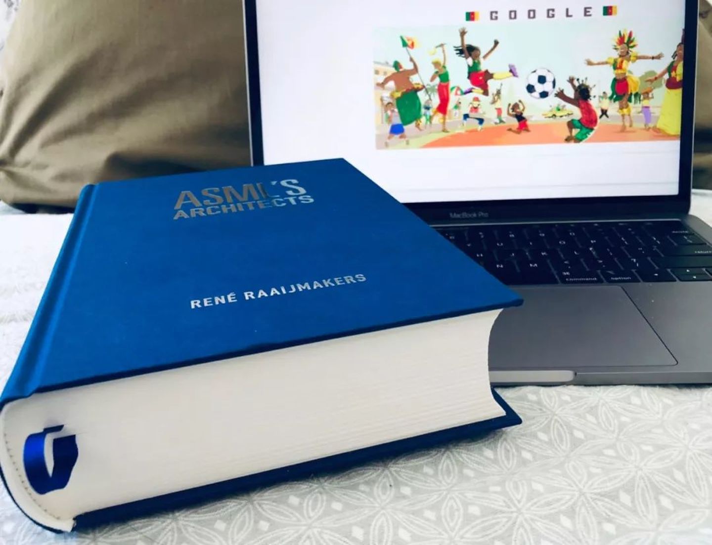
I am fortunate to have received the support of Dutch author René Raaijmakers in translating a book about the development history of the lithography machine giant ASML, entitled “ASML’s Architects”.
Author René has been contemplating this book for over fifteen years, and it took him a full seven years to write it.
Why did it take so much time to write this book? Because there was no similar book to copy from, ASML has always been a low-key company that doesn’t like to advertise.
The entire book has been translated into Chinese, with approximately 500,000 words, making it as thick as a dictionary. Every event is derived from interviews with the concerned individuals and corporate documents. Therefore, over 95% of the content is entirely fresh to Chinese readers who have never heard of it before.
René ultimately provided the answer to the question: the great contributors in the field of lithography are the ones that ought to be celebrated, and we should especially praise the courageous scientists and engineers who dare to take on challenges.
What makes me feel ashamed is that in my previous articles, I attributed all achievements simply to the company.
Next, let’s talk about some behind-the-scenes stories in the book.
Chapter Two Link to heading
Philips were quite intimidating during their joint venture with ASM.
ASM boss Arthur del Prado was born in Indonesia, which was then a Dutch colony. His father had Jewish ancestry. During World War II, when he was around ten years old, he was imprisoned in a concentration camp in Indonesia, thankfully not one under Nazi control.
Hajo Meyer, who was responsible for the early development of semiconductors at Philips, is a legend. As a Jew, he was deported from the Netherlands to Auschwitz, but he managed to escape being a victim of the gas chamber because the Germans needed him to repair machinery. He narrowly escaped again when he was forced to flee to the riverbank during the arrival of the Soviet army. Looking back, he said he almost became fertilizer or shoe polish on that occasion.
The post-war convention was for refugees to return to their place of origin. Meyer, who was thin as a pencil, walked from Poland back to the Netherlands and then went to university to study.
After the end of the Pacific War, Del Prado also returned to the Netherlands to attend university and later gained admission to Harvard Business School. At the age of 26, he traveled to Silicon Valley, where he was deeply drawn to the nascent semiconductor industry.
After graduation, Del Prado returned to the Netherlands with a small wafer and 500 dollars and founded “Advanced Semiconductor Materials” company, with ASM being the abbreviation for the company.
Chapter Three Link to heading
The level of knowledge a person possesses determines the extent of what they can achieve.
Del Prado’s company is very successful. He accurately predicted the great prospects of the chip industry and dreamed of creating a Silicon Valley in Europe. However, the arrogant Philips ignored him for many years. Del Prado wrote in the newspaper that he could easily make appointments with IBM or HP for cooperation in the United States, but it was difficult to make appointments with local giants in his hometown.
It was not until 1983, two years after ASM was listed on NASDAQ, that a Philips executive realized while reading the news that this guy had some money to talk about.
Although Del Prado pursued and negotiated for over a year, Philips still believed that ASM was too small to participate in the lithography machine market and was not optimistic about its future. Therefore, when the two parties decided to establish a joint venture (ASML), Philips cunningly utilized their 16 PAS2000 lithography machines, which were still under construction and valued at 1.8 million USD, as part of their contribution in the joint venture’s capital investment of 2.1 million USD per party.
At the time, Del Prado may not have been fully aware that these 16 PAS2000 machines were difficult to sell due to their hydraulic drive and the need for a larger power unit that caused vibration. Finding customers for these machines proved to be a challenge.
The optical components of the PAS2000 are sourced from CERCO in Paris. Although this company is strong, it cannot achieve the precision required for large-scale integrated circuits. At the time, ASML had not yet collaborated with Zeiss, and Zeiss was not interested in such a small business.
Chapter Four Link to heading
ASML was established on April Fool’s Day in 1984, the same year as Lenovo founded.
At that time, it was the heyday of Japanese semiconductors. The position of NEC and Toshiba was like that of Intel and Samsung today. The yield of DRAM produced in Japan was much higher than in the United States, which forced Intel to make drastic decisions two years later.
Behind the success of Japan’s semiconductor industry lies the photolithography techniques of two optical giants, Nikon and Canon, supported by a series of affiliated manufacturers such as Tokyo Electron, Hitachi, DISCO, Sumitomo, and Toyo Tanso.
ASML, which lacks funds and optical components, and has a zero market share, how can it compete?
During his trip to the United States for business meetings, Gjalt Smit, the first CEO of ASML, sought advice from Jim Morgan, the CEO of Applied Materials. At the time, Applied Materials was a direct competitor of ASM in the wafer front-end and back-end processes, though its size was not yet large. Smit was introduced to Morgan through a connection at Philips, and as a result, Morgan shared his thoughts candidly.
Morgan said that he definitely won’t touch photolithography, as it’s not just a process, but requires the capability to control both the machine and the light. He added that semiconductor factories usually buy photolithography equipment from one supplier, and it requires board-level decision-making.
Smit returned to his home country with a heavy heart as he had not sold a single machine.
Chapter Five Link to heading
The principle of the photolithography machine is very simple, which is to project patterns onto silicon wafers using light. However, there are two difficulties in implementation: one is how to make the patterns as small as possible, and the other is how to achieve the highest production efficiency.
How small should the pattern be? The latest technology is to have one hundred million transistors in one square millimeter (smaller than a sesame seed).
How high is the production efficiency? Currently, the core technology can produce nearly 300 pieces of 300mm wafers per hour, with thousands of chips on each wafer. ASML’s advanced lithography machines can work 24/7, with an annual unexpected shutdown time of no more than 3%.
The bald spot can only expose an area as small as a rubber stamp, 26x33mm. When exposing a wafer, it needs to be moved hundreds of times at least. One can only imagine how fast the lithography machine moves. Moreover, the positioning of each movement needs to be accurate to tens of nanometers, which is ten-thousandths of a hair strand.
Chapter Six Link to heading
ASML’s predecessors decided on the company’s main direction from the beginning, which is “precise positioning” and “speed without sacrificing accuracy”. This philosophy served as the foundation for their future success.
Making precision machinery work 7x24 hours without fail is a huge challenge in the field of engineering.
We often see news about how much nm lithography has been achieved by certain research units, but it’s important to understand that there is a huge gap between carving out two lines in a laboratory and running a factory 24/7.
The hallmark of ASML’s predecessor, the Philips NatLab, was an unwavering commitment to excellence regardless of the cost. This illustrious laboratory was the birthplace of the CD optical disc, as well as the birthplace of NXP (formerly Philips Semiconductors).
Therefore, the design principle of ASML’s lithography machines is to prioritize precision and reliability, while considering cost and price as little as possible.
ASML’s old model PAS5500 from the mid-1990s is still being refurbished and sold on their official website, which is a testament to its high reliability.
This perfectly aligns with the needs of semiconductor manufacturers, who invest billions of dollars in factories and fear nothing more than downtime. Even if the equipment is twice as expensive, as long as it can operate continuously, money can be printed continuously.
The author René also refers to the lithography machine as a License to Print Money.
Chapter Seven Link to heading
“When discussing Japanese competitors in the book, it sparked an interesting association for me (not a conclusion).”
The reason behind the decline of Japan’s semiconductor industry is not as claimed by those conspiracy theory-promoting public accounts, that it was due to the trade war.
It has no direct relation to the 1985 Plaza Accord or the Japan-US Semiconductor Agreement. By 1990, NEC, Toshiba, and Hitachi were still the top three semiconductor companies in the world, and their revenue had doubled.
In 1994, ASML only had an 18% market share, but their advanced 8-inch PAS5500 design and IPO in 1995 gave them wings. TSMC, Samsung, and Hyundai (later Hynix), who were the first to adopt this machine, quickly decided to switch almost all their photolithography to ASML.
In 1995, Toshiba, Siemens (later Infineon), and IBM formed an alliance to develop 256Mb Trench DRAM. At that time, they considered collaborating with Canon and initially did not choose ASML.
Coincidentally, Japanese semiconductor manufacturers who persistently adhered to Nikon and Canon experienced a decline lasting for a decade, while three major East Asian manufacturers who bet on ASML quickly rose and dominate the market to this day.
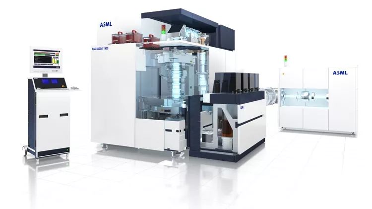
Miraculous Watershed: PAS-5500, photo from ASML’s official website.
Chapter Eight Link to heading
I reached out to some publishers in China for publishing “ASML’s Architects,” but unfortunately, most of them didn’t see any commercial value in it, even though there are no books in the market that introduce this company.
An editor from a famous university publishing house said that writing a book solely about one company would limit its sales potential, hinting that I should write a story compilation. I jokingly retorted that “Tencent’s Story” sold very well, didn’t it? He said, “That’s different.”
I suppose he might be right. Perhaps this kind of book can only sell a few thousand copies, and it’s not really profitable. Besides, today’s readers prefer fast food reading and care more about the conclusion; especially hoping to hear idols like Jack Ma tell us directly: What is the secret of success in life? Can we eat leeks? Can we win in the trade war…
However, if a book can attract young independent thinkers or semiconductor professionals who are passionate about their industry, and inspire them to delve into learning and research, there will be significant benefits for the integrated circuit industry that is strongly supported by the country.